English
 العربية
 Français
 Русский
 Español
 Português
 Deutsch
 Italiano
 日本語
日本語
 한국어
한국어
 हिन्दी

Introduction
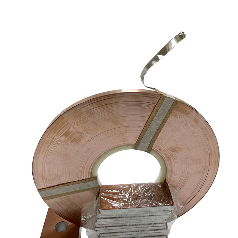
Copper-nickel clad strips combine copper’s conductivity with nickel’s weldability and corrosion resistance. Incorrect sizing leads to overheating, energy loss, poor welds, or mechanical failure. This guide covers current-carrying capability, temperature-rise limits, mechanical stiffness, weld-process compatibility, surface finish, and provides practical selection examples.
- Current-carrying capacity
- Rule of thumb: continuous current density for copper-clad strips is typically 3–5 A/mm² (adjust for cooling and installation).
- Area A (mm²) = Current I (A) / Current density J (A/mm²).
- Example: For 200 A at J = 4 A/mm² → A = 50 mm². If width = 20 mm → thickness ≈ 50/20 = 2.5 mm. In practice, use wider strips or multiple parallel strips rather than extremely thick single layers.
- Use copper effective area if nickel layer is significant.
- Temperature rise constraint
- Target: module interior ΔT ≤ 20–30 °C.
- Approximate heating: ΔT ≈ I⊃2;·R·θ_th, with R = ρ·L/A and θ_th the thermal resistance to ambient.
- Solve for A under given ΔT: A_min ≥ I·sqrt(ρ·L·θ_th / ΔT) (approximate). Apply safety factor 1.2–1.5 to account for contact resistance and pulses.
- Mechanical strength and vibration/impact
- Thin wide strips may meet electrical needs but lack stiffness. Consider:
- Increase thickness or add mechanical supports for rigidity.
- Multiple fixation points and short free spans to improve vibration resistance.
- For harsh environments, raise thickness by 10–30% or validate with vibration/drop testing.
- Weldability and process matching
- Thicker strips require higher welding energy/time.
- Welding considerations:
- Ultrasonic welding: sensitive to thickness and surface cleanliness; typically effective up to ~0.5–1.0 mm copper depending on equipment.
- Laser welding: affected by reflectivity differences between Ni and Cu; may require higher power or multiple passes for thick strips.
- Resistance/spot welding: suitable for thicker parts but watch heat transfer to cells.
- Always validate thickness vs. your welding equipment’s process window (energy, time, pressure).
- Surface roughness & cleanliness
- Contamination or oxides reduce ultrasonic and laser weld yield and increase contact resistance.
- Control surface roughness (slight roughness can aid mechanical interlock for ultrasonic), implement cleaning (solvent, plasma), and use protective packaging pre-weld.
- Typical selection cases
- 50 Ah prismatic module:
- Example: 0.2 mm × 20 mm Cu-Ni (Cu ~0.18 mm, Ni ~0.02 mm). Area 4 mm²; at 4 A/mm² supports ~16 A per strip—use multiple strips/short paths as needed.
- 100 Ah+ modules:
- Example: 0.3 mm × 30 mm (Cu ~0.28 mm, Ni ~0.02 mm). Area 9 mm²; at 4 A/mm² supports ~36 A per strip; use parallels or larger sizes for hundreds of amps.
- High-current busbars (≥200 A): use much thicker (≥1.0–2.5 mm) or wider structures with mechanical support and nickel finish for weldability/corrosion protection.
- Practical recommendations
- Balance electrical loss, hotspots, manufacturability and cost.
- Prototype with thermal imaging and vibration/thermal cycle testing.
- Confirm material specs (Ni thickness, resistivity, bonding quality) with suppliers and get samples & datasheets.
Conclusion
Start from required current and use 3–5 A/mm² to size area, then apply temperature-rise limits, mechanical and welding constraints, and verify through prototyping and testing.